Saturday, January 16, 2010

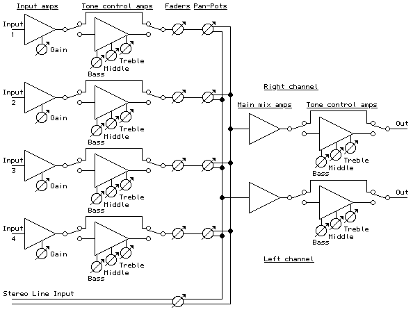
4 input mixer schematic

4 input mixer schematic


Portable Mixer

High-quality modular design

9V Battery powered - Very low current drawing

Design description:

The target of this project was the design of a small portable mixer supplied by a 9V PP3 battery, keeping high quality performance.
The mixer is formed assembling three main modules that can be varied in number and/or disposition to suit everyone needs.
The three main modules are:

Input Amplifier Module: a low noise circuit equipped with a variable voltage-gain (10 - 100) pre-set, primarily intended as high quality microphone input, also suitable for low-level line input.

Tone Control Module: a three-band (Bass, Middle, Treble) tone control circuit providing unity-gain when its controls are set to flat frequency response. It can be inserted after one or more Input Amplifier Modules and/or after the Main Mixer Amplifiers.

Main Mixer Amplifier Module: a stereo circuit incorporating two virtual-earth mixers and showing the connection of one Main Fader and one Pan-Pot.

The image below shows a Block diagram of the entire mixer featuring four Input Amplifier Modules followed by four in-out switchable Tone Control Modules, one stereo Line input, four mono Main Faders, one stereo dual-ganged Main Fader, four Pan-Pots, a stereo Main Mixer Amplifier Module and two further Tone Control Modules switchable in and out for each channel, inserted before the main Left and Right outputs.
Obviously this layout can be rearranged at everyone wish.
An astonishing feature of this design lies in the fact that a complete stereo mixer as shown below in the Block diagram draws less than 6mA current!

read more 

15 Watt Mini Amplifier

15 Watt Mini Amplifier


Notes:
This amplifier uses a dual 20 Volt power supply and delivers 15 watts RMS into an 8 ohm load. Q1 operates in common emitter, the input signal being passed to the bias chain consisting of Q8, Q9, D6, D13 and D14. Q8 and Q9 provide a constant current through the bias chain to minimize distortion, the output stage formed by a discrete darlington pair (Q2,Q4) and (Q7,Q11). The last two transistors are power Transitors, specifically the 2N3055 and MJ2955. The 7.02K resistor, R16 was made using a series combination of a 4.7K, 680 Ohms, and two 820 Ohms. The 1.1K resistor, R3 was made using a 100 Ohms and a 1K resistor. You can use this circuit with any walkman or CD player since it is designed to take a standard 500mv RMS signal.

0 - 300V Adjustable Power Supply

0 - 300V Adjustable Power Supply


Introduction


To prevent my high voltage experiments to go up in smoke completely, I designed
a simple circuit which can provide an adjustable voltage source of 0 to 330 Volt..
The supply is short-ciruit proof: the current is limited to about 100mA.

Circuit description

TR1 is a 1:1 mains transformer; it is included for safety.

The mains voltage from TR1 is rectified with bridge D1 (1Amp / 500V) and large elcap C1.

T1 is switched as a source follower: the source of T1 will follow the voltage of the
wiper of R3. D2 is included to protect the gate of T1; although in theory not necessary
I strongly recommend to include it!

T2 and shunt resistor R2 build the current limiter. When the output current becomes too high, T2 will discharge
the gate of T1. This will prevent the current to become too high.
The value of R3 has been determined experimentally; it depends also on the Hfe of T2 so you may need to tune the value of R2.

Note that T1 needs a large heatsink: in worst case T1 will dissipate 330V x 100mA = 33Watt!
Instead of a BUZ 326 (400V/10.5Amp) you can also use an IRF740 (400V/10Amp).
The output impedance of the power supply is determined by the beta of T1, so the larger the MOSFET
the lower the output impedance!


power supply schematic - 12 Volt 30 Amp Power Supply

power supply schematic - 12 Volt 30 Amp Power Supply

Description
Using a single 7812 IC voltage regulator and multiple outboard pass transistors, this power supply can deliver output load currents of up to 30 amps. The design is shown below:


Notes
The input transformer is likely to be the most expensive part of the entire project. As an alternative, a couple of 12 Volt car batteries could be used. The input voltage to the regulator must be at least several volts higher than the output voltage (12V) so that the regulator can maintain its output. If a transformer is used, then the rectifier diodes must be capable of passing a very high peak forward current, typically 100amps or more. The 7812 IC will only pass 1 amp or less of the output current, the remainder being supplied by the outboard pass transistors. As the circuit is designed to handle loads of up to 30 amps, then six TIP2955 are wired in parallel to meet this demand. The dissipation in each power transistor is one sixth of the total load, but adequate heat sinking is still required. Maximum load current will generate maximum dissipation, so a very large heat sink is required. In considering a heat sink, it may be a good idea to look for either a fan or water cooled heat sink. In the event that the power transistors should fail, then the regulator would have to supply full load current and would fail with catastrophic results. A 1 amp fuse in the regulators output prevents a safeguard. The 400mohm load is for test purposes only and should not be included in the final circuit. A simulated performance is shown below:


Calculations
This circuit is a fine example of Kirchoff's current and voltage laws. To summarise, the sum of the currents entering a junction, must equal the current leaving the junction, and the voltages around a loop must equal zero. For example, in the diagram above, the input voltage is 24 volts. 4 volts is dropped across R7 and 20 volts across the regulator input, 24 -4 -20 =0. At the output :- the total load current is 30 amps, the regulator supplies 0.866 A and the 6 transistors 4.855 Amp each , 30 = 6 * 4.855 + 0.866. Each power transistor contributes around 4.86 A to the load. The base current is about 138 mA per transistor. A DC current gain of 35 at a collector current of 6 amp is required. This is well within the limits of the TIP2955. Resistors R1 to R6 are included for stability and prevent current swamping as the manufacturing tolerances of dc current gain will be different for each transistor. Resistor R7 is 100 ohms and develops 4 Volts with maximun load. Power dissipation is hence (4^2)/200 or about 160 mW. I recommend using a 0.5 Watt resistor for R7. The input current to the regulator is fed via the emitter resistor and base emitter junctions of the power transistors. Once again using Kirchoff's current laws, the 871 mA regulator input current is derived from the base chain and the 40.3 mA flowing through the 100 Ohm resistor. 871.18 = 40.3 + 830. 88. The current from the regulator itself cannot be greater than the input current. As can be seen the regulator only draws about 5 mA and should run cold.

power supply schematic - Gyrator Circuit

power supply schematic - Gyrator Circuit


Description
An electronic recitification circuit. The use of large, heavy and expensive electrolytic capacitors is avoided, being replaced by an active transistor in this gyrator circuit.


Circuit Notes
To avoid excess ripple output on a power supply feeding a heavy load, usually a large value capacitor is chosen following the rectifier. In this circuit, C1's value is only a 470uF. The gyrator circuit works on the principle that the value of input capacitance at the base-emitter terminals of a transitor is effectively multiplied by the static forward current gain, HFE of the transistor. In this circuit C2, a 100uF capacitor is effectively magnified at the ouput ( Vreg ).

If you assume a dc current gain, HFE of 50 for the 2N3055 power transistor, then the effective value of the smoothing capacitor would be 50x this value; or be the same as using a 5000uF capacitor without the power transistor. The graph below shows the output voltage and current through the load :-


The load draws nearly 400mA. With the output directly from the rectifier there is about 5v pk-pk ripple in the output. Using the output at the emitter of the transistor things are much better. The circuit will take a few hundred milliseconds for the output voltage to stabilize and reach maximum value. The advantages are that a smaller, less costly reservoir capacitor can be used with this circuit to give a high quality

100W Guitar Amplifier

100W Guitar Amplifier


Guitar amplifiers are always an interesting challenge. The tone controls, gain and overload characteristics are very individual, and the ideal combination varies from one guitarist to the next, and from one guitar to the next. There is no amp that satisfies everyone's requirements, and this offering is not expected to be an exception. The preamp is now at Revision-A, and although the complete schematic of the new version is not shown below, the fundamental characteristics are not changed - it still has the same tone control "stack" and other controls, but now has a second opamp to reduce output impedance and improve gain characteristics.


One major difference from any "store bought" amplifier is that if you build it yourself, you can modify things to suit your own needs. The ability to experiment is the key to this circuit, which is although presented in complete form, there is every expectation that builders will make modifications to suit themselves.

The amp is rated at 100W into a 4 Ohms load, as this is typical of a "combo" type amp with two 8 Ohm speakers in parallel. Alternatively, you can run the amp into a "quad" box (4 x 8 Ohm speakers in series parallel - see Figure 5 in Project 27b, the original article) and will get about 60 Watts. For the really adventurous, 2 quad boxes and the amp head will provide 100W, but will be much louder than the twin. This is a common combination for guitarists, but it does make it hard for the sound guy to bring everything else up to the same level.
read more

Friday, January 15, 2010

datasheet 2n2222a

datasheet 2n2222a

download

Related Keywords:

2N2222A Datasheet 2N2222A Data Sheet 2N2222A Application Note 2N2222A Equivalent 2N2222A Replacement


2N2222A Fiche technique 2N2222A Scheda 2N2222A Ficha técnica de 2N2222A équivalent 2N2222A gleichwertige

2N2222A Schematische 2N2222A Schéma 2N2222A Schematische 2N2222A Schematico 2N2222A Esquema

2N2222A Component 2N2222A Reference Design 2N2222A Schematic 2N2222A Distributor 2N2222A Specs

2N2222A equivalente 2N2222A Ersatz 2N2222A remplacement 2N2222A Mechanical Outline 2N2222A Features

2N2222A Example 2N2222A RoHS 2N2222A Design 2N2222A Circuit 2N2222A Technical Specs

2N2222A Errata 2N2222A User Guide 2N2222A Archive 2N2222A Datenblatt 2N2222A Ficha técnica

2N2222A Prototype 2N2222A Design Idea 2N2222A Samples 2N2222A Inventory 2N2222A Stock

2N2222A Revision 2N2222A Product Brief 2N2222A Release Notes 2N2222A Cross Reference 2N2222A MOQ

2N2222A Lead Time 2N2222A Leadtime 2N2222A Xref 2N2222A Prototyping 2N2222A PDF

2N2222A Capacity 2N2222A Availability 2N2222A Broker 2N2222A Distribution 2N2222A Catalog

2N2222A EOL 2N2222A End-of-Life 2N2222A PCN 2N2222A Process Change Notification 2N2222A Explanation

2N2222A Description 2N2222A Feature 2N2222A Operating Parameter 2N2222A Suffix 2N2222A Options

2N2222A Pin-out 2N2222A Marking Code 2N2222A Electrical Characteristics

Popular Posts